Can I Add External SRAM to My A7 Design?

Although the A7 directly supports low-cost, high-performance SDRAM, some applications require an external SRAM interface.  This article describes how to build such an interface.


NOTE

If you are creating an external SRAM memory interface that shares the A7’s memory interface unit, the data width of the external SRAM memory interface must match that of the external Flash interface.  For example, if the Flash interface is 16-bits wide, then the SRAM interface must also be 16-bits wide.  The SRAM interface cannot have a data width different than the Flash interface.

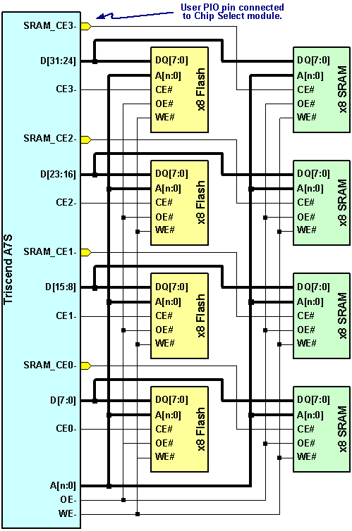
In this example, assume that the application has 2Mx32 of Flash for code and configuration storage and 8Mx32 of SRAM, as shown in Table 1.  Both the Flash and SRAM interfaces are built from four byte-wide devices.

Table 1.  Memory Connected to A7 Example Design.

Memory Subsystem

Architecture

Memory Devices

Flash

2Mx32

4x512Kx8

SRAM

8Mx32

4x2Mx8


Figure 1 shows the connections between the A7S device and the external Flash and SRAM.  The Flash devices connect directly to the A7’s memory interface unit (MIU) signal.  The SRAM interface shares a majority of signals, including the address, data, output enable, and write-enable signals.  The only unique signals between the Flash and SRAM are the chip-enable signals.

Schematic diagram showing the connections between a Triscend A7S device and to both a 32-bit Flash interface and a 32-bit SRAM interface.  In this example, all memory devices are byte-wide.

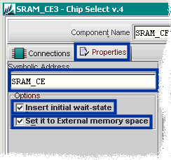
Figure 1.  An example A7 interface to both external Flash and external SRAM.

The four byte-wide Flash devices are separately enabled using the A7’s dedicated CE3- through CE0- outputs.  These four enables allow byte, half-word, and word-wide transactions to the Flash.  The timing for Flash transactions is controlled by the MIU itself.  When you select a specific Flash device and speed grade during configuration, FastChip automatically configures the MIU timing for you.

The four byte-wide SRAM devices are separately enable, but using logic created in the CSL matrix.  In specific, the Chip Select soft IP module provides a convenient way to create the individual chip-enable outputs.  Using the Set it to External memory space option, the SRAM devices can share most of the MIU’s signals.  However, the memory access timing is controlled by the other CSL logic.

Let’s build the interface.

1. Start FastChip and choose a Chip Select v.4 module from FastChip’s soft IP module library.  Type SRAM_CE3 for the Component name and type SRAM_CE3_ for the chip-select output name.

Enter the Component Name and Chip Select output names on the Chip Select module.

2. Click Properties and type SRAM_CE for the Symbolic Address.  In this example, we want the external SRAM interface to share some of the memory interface unit (MIU) signals.  Check Set it to External memory space.  This option turns on the MIU’s address, data, output-enable, and write-enable signals whenever this chip-select module is addressed over the CSI bus.

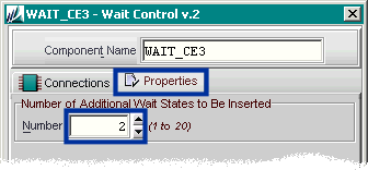
In this example, assume that the SRAM requires four clock cycles for each access.  Because we need at least one wait-state to meet this requirement, check Insert initial wait-state.  The additional two wait-states will be added later using another soft IP module.

On the Chip Select module, click Properties and enter the symbolic address.  Check both the "Insert initial wait-state" and "Set it to External memory space" options.

3. Assign the address region for the SRAM interface.  In this example, assume that the SRAM occupies the 8Mbyte region between 0x2000_0000 and 0x2100_0000.  To specify this region, click Advanced Addressing under Addressing Mode.  Type in the starting CSI address as 2000_0000.  The address mask determines the size of the address region decoded.  The region is 8Mbytes and we want all higher-order address lines decoded. Type FF80_0000 for the Address Mask.


NOTE

You can choose any CSI bus starting address as long as it does not conflict with the A7’s overall memory map.  See Figure 28 in the A7 data sheet.

Choose the "Advanced Addressing Mode" and specify the starting CSI address and address mask.  Set the appropriate "Lane Sensitivity".

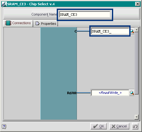
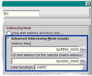
For SRAM_CE3-, we want this Chip Select module to respond to all transactions that require byte lane B3.  Set Lane Sensitivity to LANEB3.  As shown in Table 2, this Chip Select module with then respond to all word-wide transactions, all transactions to the high half-word, and all transactions by byte-lane 3.  Click OK when finished.

Table 2.  Byte Lanes and Response to Various Transaction Sizes.


D[32:24]

D[23:16]

D[15:8]

D[7:0]

Byte Lane

B3

B2

B1

B0

Word


High Half-word


Low Half-word


Byte B3


Byte B2


Byte B1


Byte B0


4. Repeat Steps 1 through 3 to create similar logic for SRAM_CE2-, SRAM_CE1-, and SRAM_CE0-.  Be sure to set the proper byte lane sensitivity.

5. In this example, the SRAM requires four clock cycles per access, requiring three wait-states on the CSI bus during a transaction.  The Chip Select module asserts the first wait-state whenever it is addressed over the bus.  Checking the Insert initial wait-state causes this initial wait-state.  A separate soft IP module asserts the two additional wait-states required.

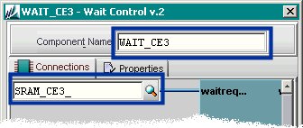
Choose the Wait Control v.2 module from the FastChip library.  Type WAIT_CE3 for the Component Name.  Connect the “waitreq” wait request input to the output of the chip select module by typing SRAM_CE3_ or choosing the signal from FastChip’s Connection Port chooser.

Connect the wait request input to the output of the Chip Select module.

6. Click Properties and set the number of additional wait-states to 2.  Click OK when finished.

Whenever a bus master addresses the associated Chip Select module, the module will insert an initial wait-state followed by two additional wait-states inserted by Wait Control module, for a total period of four CSI bus cycles.

Click Properties and enter the appropraite number of additional wait-states.

7. Each Chip Select module requires a corresponding wait-state generator.  Repeat Steps 5 and 6 for the other chip select signals.

8. Connect the chip-select signals to associated output pins.  Select an Output v.2 module from the FastChip library.  Type SRAM_CE for the Component Name.  Increase the Component Width to 4.

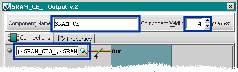
The outputs from the Chip Select modules are active-High.  The external memory requires an active-Low signal.  Connect the outputs from the Chip Select modules to the Output module.  Invert each signal by prepending the signal name with a tilde (~), indicating that the signal is inverted.

The Out port of the module expects four signals.  Type {~SRAM_CE3_,~SRAM_CE2,~SRAM_CE1,~SRAM_CE0} to create a four-signal connection, inverting each of the signals.

The outputs from the Chip Select modules are all active-High.  Invert them in the Output module.

9. Click Properties.  Set the Output Buffer Slew Rate Control to Fast to minimize the chip select delay.  If the design will operate in power-down mode, select Output active during power-down to pull the SRAM’s CE# pins High to prevent spurious reads or writes.  Click OK when finished.

Choose the Fast output option for best performance.  Be sure that the SRAM CE# pins are held High when in power-down mode.

 Invoke the I/O Editor either by selecting Constraints à I/O Editor from the FastChip menu or by clicking the FastChip button in the toolbar.

Click the I/O Editor button in the FastChip toolbar.

 Click the MIU button from the I/O Editor toolbar.

Click the MIU button in the I/O Editor toolbar.

 Because both the Flash and SRAM interfaces are 32-bit wide, but use byte-wide memory devices, enable all four chip-enable signals by checking CEN[1], CEN[2], and CEN[3].

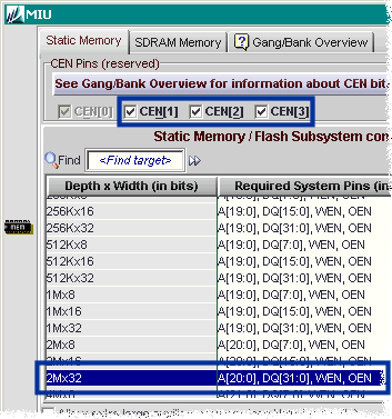
Set the data width for the MIU interface to 2Mx32.  This action reserves the proper number of address, data, and control signals on the A7 device.  Again, the data width of the external Flash and SRAM memory interfaces must be identical.

Enable all the chip-enable signals.  Set the depth and width of the external memory interface.

 If adding an external SRAM, be sure to disable the SDRAM memory interface.  The extra loading of the SRAM devices on the MIU interface may violate the timing requirements for an SDRAM interface.  Do not use both an external SRAM and external SDRAM interface in the same application.

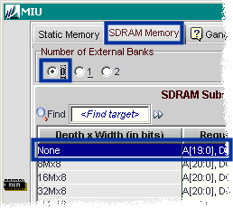
Click SDRAM Memory.  Set the number of external banks to 0.  Set the Depth x Width of the SDRAM interface to None.  Click OK when finished.

If interfacing to external SRAM, be sure to disable the external SDRAM interface.


FastChip Version: 2.4.0

This solution may or may not apply to other versions of the FastChip development system.


Triscend logo.®

© 2002 by Triscend Corporation.  All rights reserved.